


- Measurements of the Temperature Coefficient of Resistance of CVD-Grown Graphene Coated with PEI
Soomook Lim*, Ji Won Suk*†
* School of Mechanical Engineering, Sungkyunkwan University, Korea
- PEI가 코팅된 CVD 그래핀의 저항 온도 계수 측정
임수묵*· 석지원*†
This article is an open access article distributed under the terms of the Creative Commons Attribution Non-Commercial License (http://creativecommons.org/licenses/by-nc/4.0) which permits unrestricted non-commercial use, distribution, and reproduction in any medium, provided the original work is properly cited.
There has been increasing demand for real-time monitoring of body and ambient temperatures using wearable devices. Graphene-based thermistors have been developed for high-performance flexible temperature sensors. In this study, the temperature coefficient of resistance (TCR) of monolayer graphene was controlled by coating polyethylenimine (PEI) on graphene surfaces to enhance its temperature-sensing performances. Monolayer graphene grown by chemical vapor deposition (CVD) was wet-transferred onto a target substrate. To facilitate the interfacial doping by PEI, the hydrophobic graphene surface was altered to be hydrophilic by oxygen plasma treatments while minimizing defect generation. The effect of PEI doping on graphene was confirmed using a back-gated field-effect transistor (FET). The CVD-grown monolayer graphene coated with PEI exhibited an improved TCR of -0.49(±0.03) %/K in a temperature range of 30~50oC
최근 웨어러블 소자를 이용한 신체와 주변 온도의 실시간 모니터링에 대한 수요가 급격히 증가하고 있다. 그래핀 기반 써미스터가 고성능 유연 온도 센서로 개발되어 왔다. 본 연구에서는 단일층 그래핀의 온도 측정 성능을 개선하기 위하여 표면에 polyethylenimine(PEI)를 코팅하여 저항 온도 계수(TCR)를 조절하였다. 화학기상증착법(CVD)에 의해 합성한 단일층 그래핀은 습식 전사 공정을 통해 원하는 기판에 전사되었다. PEI에 의한 계면 도핑을 유도하기 위하여, 소수성의 그래핀 표면을 산소 플라즈마 처리를 통해 결함을 최소화하면서 친수성으로 제어하였다. PEI 도핑 효과를 전계효과트랜지스터(FET)를 이용하여 확인하였다. PEI 도핑에 의해서 CVD 그래핀의 TCR 값이 30~50oC의 온도 범위에서 -0.49(±0.03)%/K로 향상된 것을 확인하였다
Keywords: 그래핀(Graphene), 저항 온도 계수(Temperature coefficient of resistance), 도핑(Doping), 온도 센서(Temperature sensor)
인간의 활동과 상태를 모니터링하고 보조할 수 있는 웨어러블 장치에 대한 수요가 급증하고 있다[1-5]. 특히 표면 온도를 관측하는 것은 신체 상태와 주변 환경의 변화를 반영할 수 있기 때문에 중요한 감지 작업 중 하나이다[6,7]. 웨어러블 장치에 적용될 온도 센서는 시스템의 표면에 부착되고 시스템의 움직임에 따라 변형되어야 하므로 유연해야 하며 미세한 온도 변화를 감지할 정도의 높은 민감도가 요구된다[8,9]. 온도 감지를 위한 메커니즘은 열 저항 및 열전 효과가 주로 사용되고 있으며, 이 중 열에 의한 저항 변화를 측정하는 열 저항 기반 온도 센서는 금속 등이 사용되었으나 기계적 유연성의 한계로 인해 새로운 유연 소재의 필요성이 대두되고 있다[10].
2차원 탄소소재인 그래핀은 기계적, 열적, 전기적 특성이 우수하고 유연성이 뛰어나 전자 피부, 유연 장치 등 차세대 소자에 필요한 신소재로 주목받고 있다[11-17]. 다양한 전자 소자로 응용하기 위하여, 그래핀의 전기적 특성을 제어할 필요성이 있으며, 도핑은 그 대안 중 하나로, 탄소 원자를 헤테로 원자로 대체하는 치환 도핑과 그래핀 표면에 도펀트를 물리적 또는 화학적으로 흡착시키는 계면 도핑에 대한 연구가 진행되었다[18-20]. 계면 도핑의 경우 그래핀의 소수성 표면 특성으로 인해 도펀트의 물리적 흡착이 제한적으로 이뤄질 것으로 예상된다. 이에 그래핀의 표면 특성이 계면 도핑에 미치는 영향을 조사할 필요가 있다.
더불어, 열 저항 기반 온도 센서에서 금속성 소재들은 전자 산란에 의해 온도와 저항이 비례하는 positive temperature coefficient(PTC) 특성이 나타나는 반면 반도체 소재들은 열적으로 활성화된 캐리어의 증가로 인해 온도와 저항이 반비례하는 negative temperature coefficient(NTC) 특성이 나타난다[21]. 이에 그래핀 기반 고성능 써미스터 개발을 위해선 도핑에 따른 그래핀의 전자 특성이 temperature coefficient of resistance(TCR)에 미치는 영향을 이해할 필요가 있다.
이에 본 연구에서는 산소 플라즈마를 이용하여 그래핀 표면 특성을 조절하였으며 polyethylenimine(PEI)를 이용한 계면 도핑 시 표면 특성에 따른 도핑 효과의 차이를 field-effect transistor(FET)를 통해 확인하였다. 또한 PEI가 흡착된 그래핀의 TCR을 측정하였으며 향상된 도핑 효과로 인한 TCR의 개선을 확인하였다.
2.1 그래핀 합성 및 습식 전사
단일층 그래핀은 구리 포일(Thermo Fisher Scientific) 위에 저압 화학기상증착법(CVD)을 통해 합성되었다. 1000oC 수소 분위기에서 한 시간 열처리한 후, 메탄과 수소가 혼합된 가스 분위기에서 15분 동안 그래핀을 합성하였다[22,23]. 그래핀을 기판에 전사하기 위하여, 구리 포일에 합성한 그래핀 위에 클로로벤젠에 녹인 poly(methyl methacrylate) (PMMA, 15 mg/mL, Sigma-Aldrich) 용액을 스핀 코팅하였다. PMMA가 코팅된 그래핀/구리 포일을 과황산암모늄 용액 표면에 띄워 구리 포일을 식각한 후 기판(SiO2/Si 또는 polyethylene terephthalate(PET))에 습식 전사하였다[24,25]. 기판과 그래핀의 접착력을 높이기 위하여 140oC에서 2시간 열처리한 후, 아세톤으로 PMMA를 제거하였다.
2.2 그래핀의 표면 처리 및 계면 도핑
기판에 전사된 그래핀에 대해 산소 플라즈마 처리를 통해 표면 친수성을 조절하였다. 입력 파워와 산소 유량을 각각 100 W, 10 sccm으로 고정하고 처리 시간을 조정하였다. 그래핀 식각을 방지하기 위해 기판을 뒤집어서 처리하였으며 그래핀과 바닥사이의 간격은 1 mm로 고정하였다(Fig. 1(a)).
계면 도핑을 위해 PEI(Sigma-Aldrich)를 플라즈마 처리한 그래핀 표면에 딥 코팅하였다. 딥 코팅 공정에서 회수 속도와 두께는 상관관계를 가지며, 0.1~1 mm/sec 속도에서 최소 두께가 얻어지는 것으로 보고되었다[26]. 초박형 폴리머 층을 코팅하기 위해 에탄올에 1 wt%로 PEI를 녹인 후, 그래핀을 1.5 mm/sec의 속도로 담그고 3분 후 0.5 mm/sec 속도로 빼냈다(Fig. 1(b)). 산소 플라즈마 처리로 생성된 산소 작용기는 낮은 공기 안정성을 가져 플라즈마 처리 직후 PEI 코팅을 진행했다[27].
2.3 그래핀의 특성 분석
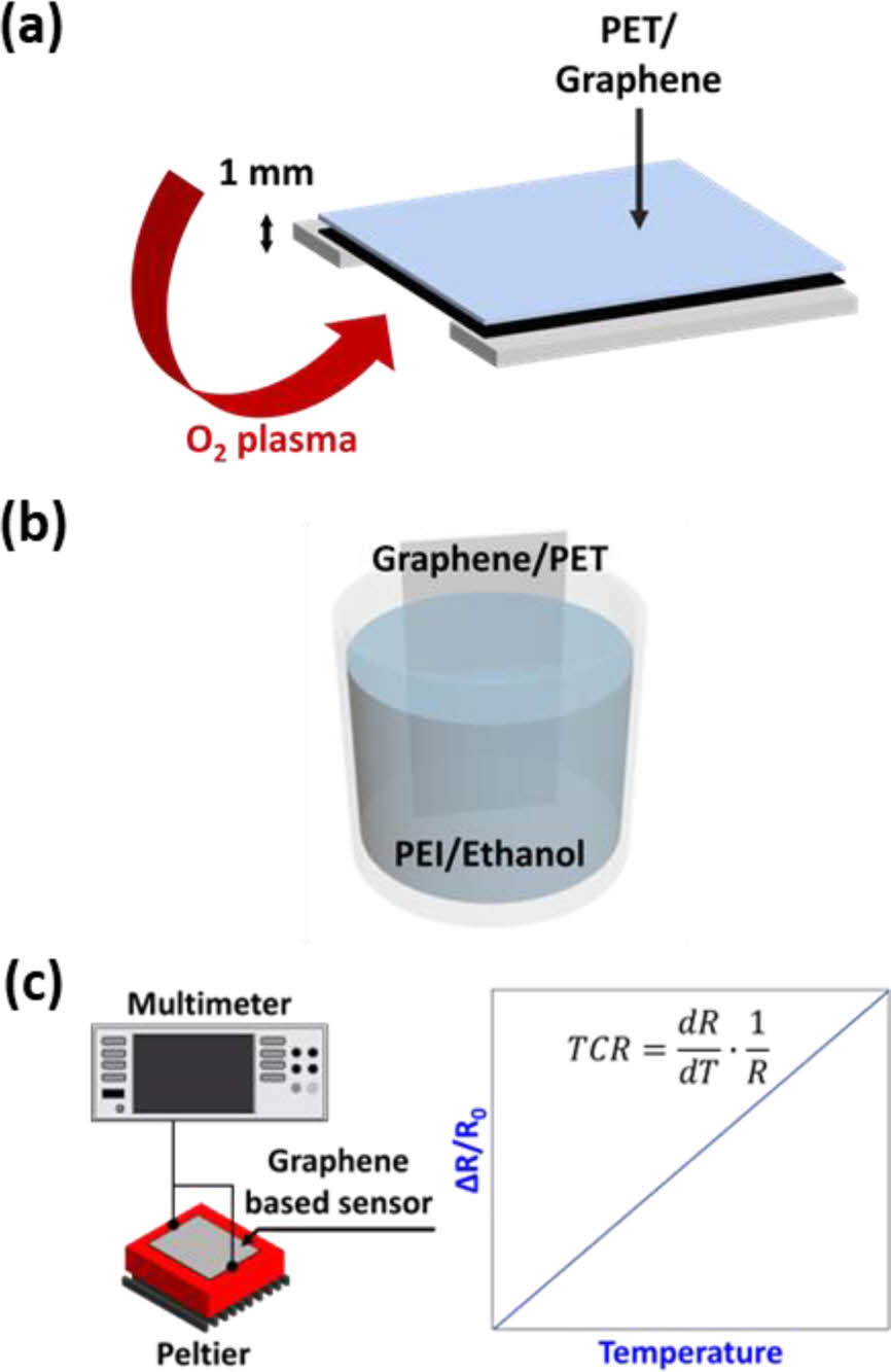
주사전자현미경(scanning electron microscope (SEM), Jeol)을 이용하여 그래핀의 표면을 관찰하였다. 표면 처리에 따른 화학 구조 변화는 405 nm 파장의 라만 분광기(Nanobase)를 사용하여 관찰하였다. 추가적으로 표면 처리 및 계면 도핑에 따른 특성 분석을 위해 FET를 제작하였다. SiO2/Si 기판(285 nm 두께의 SiO2와 비저항이 0.001-0.005 Ω·cm인 Si)을 백게이트로 사용하고 소스/드레인 전극(Cr(10 nm)/Au(40 nm))을 포토리소그래피 및 스퍼터링 공정을 통해 기판 위에 제작했다[28]. FET 소자의 전류-전압 특성은 소스미터(Keithley)에 0.1 V를 인가하여 측정하였으며 모든 측정은 실온 및 대기 중에서 수행되었다.
2.4 저항 온도 계수(TCR) 측정
열저항의 감도는 TCR로 대표되며 아래와 같이 정의된다[29].
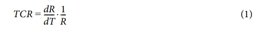
이때 dR, dT, R는 각각 저항 변화, 온도 변화, 초기 저항을 의미한다. TCR 측정은 기판의 열전달 이슈를 최소화하기 위하여 두께가 얇은 고분자 필름(PET)에 전사된 그래핀을 사용하였으며 이 때 시료의 크기는 2.5 cm × 1.5 cm이다. Fig. 1(c)와 같이 센서를 열원과 접촉시키고 30~50oC로 조정하면서 멀티미터(Keithley)를 통해 저항 변화를 측정하였다.
|
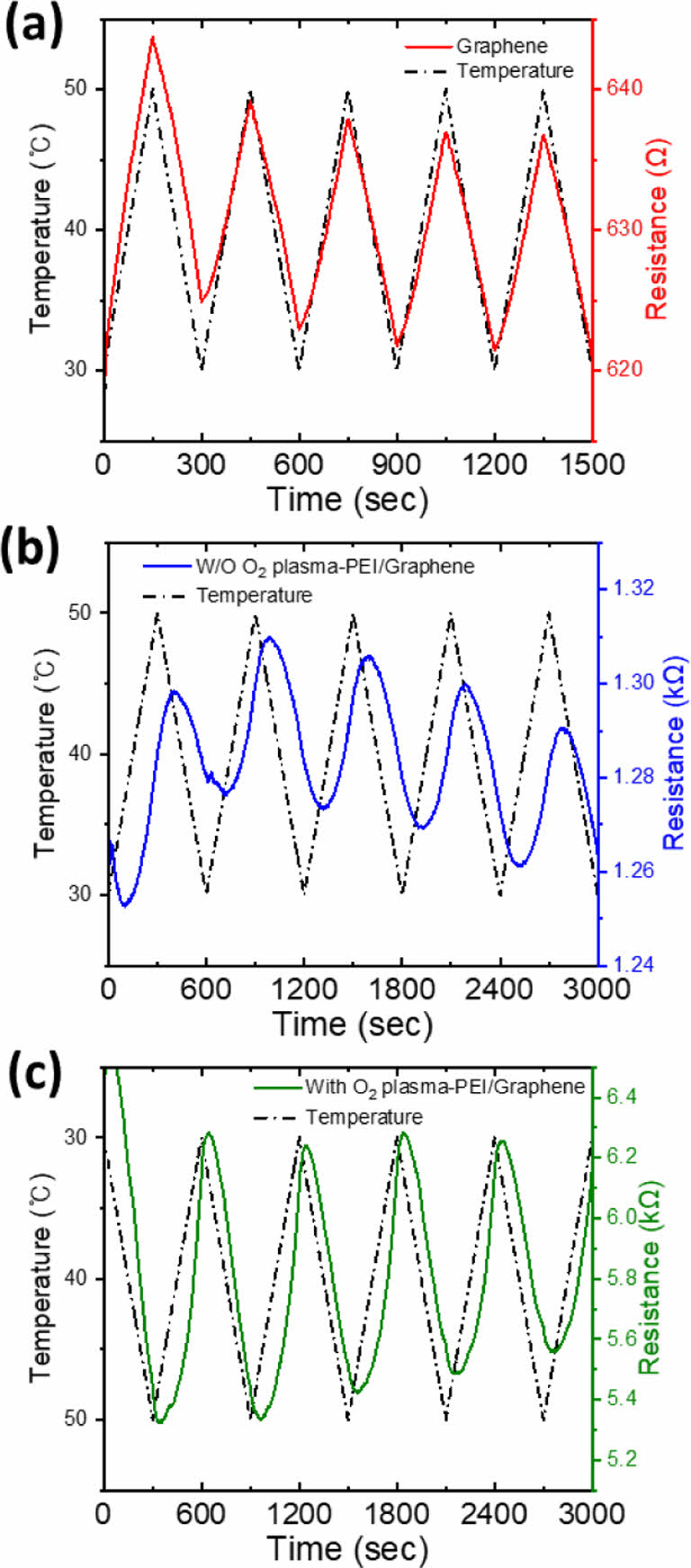
Fig. 1 (a, b) Schematic of the sample preparation. (a) Oxygen plasma treatment. (b) Dip coating process. (c) Characterization of graphene temperature sensors by controlling temperature with Peltier and measuring the resistance change of graphene with a multimeter |
Fig. 2(a)는 SiO2/Si 기판 위에 전사된 그래핀의 SEM 이미지이다. 단일층의 그래핀이 균일하고 연속적으로 합성되었으며, 작은 다층 그래핀 부분이 존재하는 것을 확인할 수 있다. Fig. 2(b)는 그래핀의 라만 분석 결과이다. 합성된 그래핀은 ~1600 cm-1에 위치하는 G 밴드와 ~2700 cm-1에 위치하는 2D 밴드가 뚜렷하게 보이며, G 밴드 peak 강도에 대한 2D 밴드의 peak 강도 비율이 3.2 ± 0.7로 나타났다. 이를 통해 단일층 그래핀이 합성되었음을 확인할 수 있으며, ~1350 cm-1에 위치하는 D 밴드가 없어 결함이 낮은 고품질 그래핀임을 알 수 있다[30,31]. 산소 플라즈마 처리 시간에 따른 그래핀의 표면 변화를 라만 분석을 통해 확인하였다. 표면 처리 시간이 9초 이상일 때 구조적 결함을 의미하는 D 밴드가 증가하기 시작하였다. 이는 산소 플라즈마 처리를 통해 그래핀 표면에 산소 작용기를 유도할 수 있음을 나타내며, 이를 통해 그래핀 표면이 소수성에서 친수성으로 변하는 것을 의미한다. 산소 플라즈마를 21초 동안 처리하는 경우 비정질 탄소 구조에서 나타나는 D’ 밴드(~1620 cm-1)가 관측되었다[32,33]. 라만 분석과 더불어, 표면 처리가 그래핀의 전기적 특성에 미치는 영향을 관측하기 위해 산소 플라즈마 처리 시간에 따른 면저항을 측정하였다(Fig. 2(c)). 9초 처리의 경우 라만 분석에서 구조적 결함을 확인하였지만, 면저항이 크게 증가하지 않았다. 그러나, 21초 이상 플라즈마 처리를 하는 경우, 면저항이 86.0(±13.2)kΩ/sq로 크게 증가하는 것을 알 수 있다. 라만 분석과 면저항 측정을 통해서, 산소 플라즈마 처리를 통해 산소 작용기 유도가 가능하지만, 과도하게 플라즈마 처리를 하게 되면 그래핀의 결함이 크게 증가하여 저항 변화 온도 센서로 사용하기 어려운 것을 알 수 있다. 따라서, 본 연구에서는 표면 결함을 최소화하면서 전기적 특성을 유지하고 친수성 표면을 가질 수 있는 조건인 9초의 표면 처리 시간을 사용하였다.
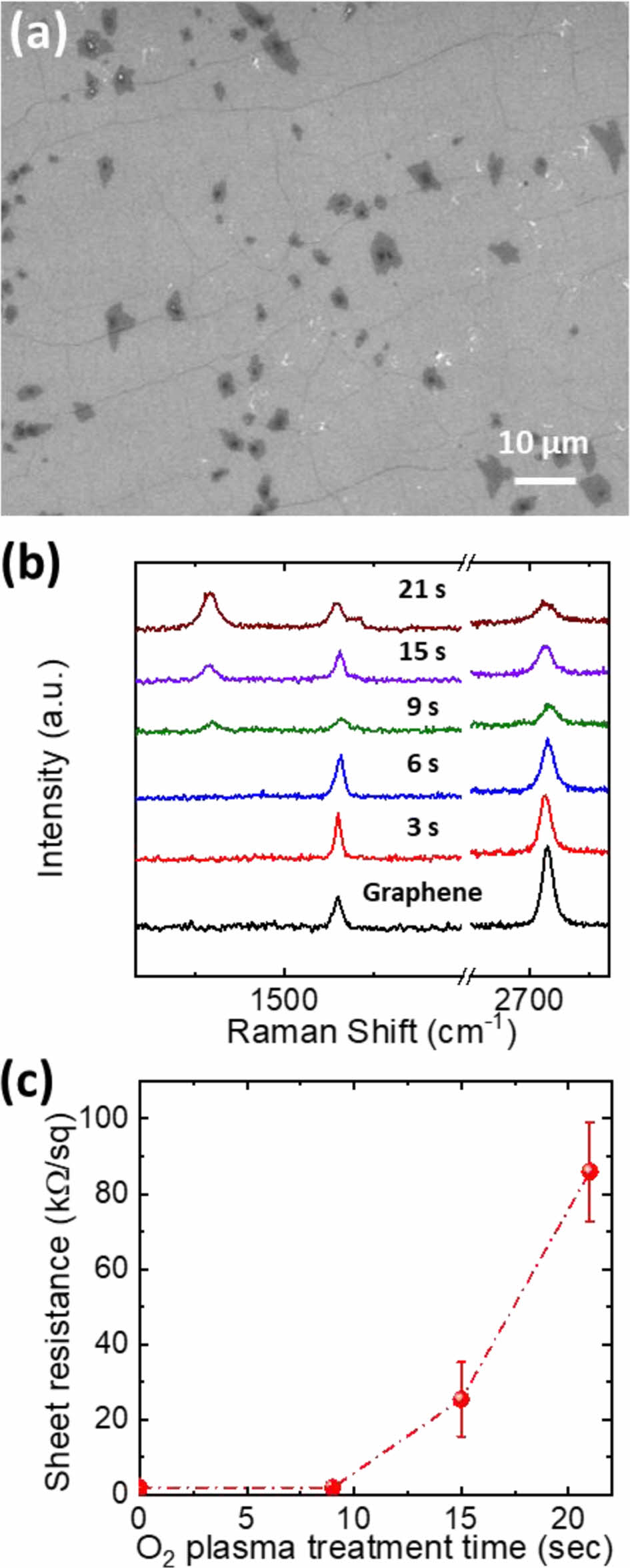
Fig. 3(a, b)는 각각 그래핀의 표면 처리 및 계면 도핑에 따른 FET 측정 결과와 그에 따른 Dirac point voltage 분포도이다. 습식 전사된 그래핀은 PMMA 잔류물 및 대기 중 산소 흡착으로 인해 p형 도핑되어 52(±9)V의 Dirac point voltage를 나타내었다[34]. 산소 플라즈마 처리된 그래핀은 Dirac point voltage가 92(±18)V로 증가하였는데, 이는 산소 플라즈마 처리에 의해 그래핀 표면에 형성된 산소 작용기로 인해 p형 도핑이 증가하였기 때문인 것으로 보인다[35]. 반면, 플라즈마 처리없이 PEI를 코팅한 경우, 그래핀 FET 소자의 Dirac point voltage가 -17(±22)V로 이동하였으며 이는 그래핀 표면에 흡착된 n형 도펀트인 PEI의 전자 공유로 인해 그래핀의 캐리어 유형이 n형으로 변화된 것을 의미한다[34]. 산소 플라즈마 처리 후 PEI가 코팅된 그래핀의 경우 Dirac point voltage가 -71(±13)V로 나타났다. 이는 산소 플라즈마 처리로 인해 소수성 그래핀 표면이 친수성으로 변하여, Fig. 3(c)의 모식도와 같이 수용액 형태의 PEI 용액 코팅이 보다 균일하게 이루어진 결과로 보인다. 따라서, PEI 코팅을 통해 n형 도핑을 유도하기 위해서는 산소 플라즈마 처리를 이용하여 그래핀 표면을 친수성으로 조절하는 것이 유효함을 확인하였다.
그래핀 표면 처리에 따른 도핑 효과의 차이가 그래핀의 TCR에 미치는 영향을 조사하였다. Fig. 4는 시간에 따라 열원의 온도를 주기적으로 변화하면서, 그래핀의 저항 변화 응답을 관찰한 결과이다. 그래핀은 기판과의 계면 전자-포논 산란으로 인해 PTC 특성이 나타났다(Fig. 4(a)). 산소 플라즈마 처리를 하지 않고 그래핀에 PEI를 코팅한 경우, 앞서 Fig. 3에서 살펴본 바와 같이 PEI의 흡착 면적이 작아서 PEI 도핑 효과가 뚜렷하게 나타나지 않았다(Fig. 4(b)). 반면에, 산소 플라즈마 처리 후 PEI 코팅을 한 경우, NTC 특성이 나타났다(Fig. 4(c)). 이는 균일하게 코팅된 PEI가 장거리 산란에 의해 NTC 특성을 유도한 것으로 보인다[36,37].
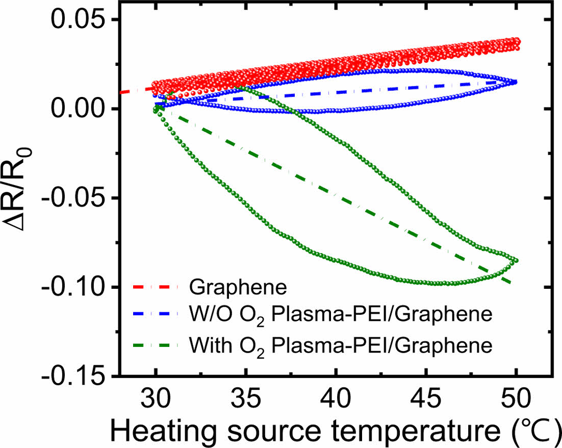
Fig. 4로부터 그래핀의 온도 변화에 따른 저항 변화 그래프를 얻어 CVD 합성된 단일층 그래핀의 TCR을 측정하였다(Fig. 5). PET 위에 습식 전사 후, 추가적인 처리를 하지 않은 단일층 그래핀은 0.11(±0.03)%/K의 TCR을 나타냈다. 이전 연구에서 측정한 단일층 그래핀의 TCR은 0.09~0.42%/K이며 기판에 따른 계면 전자-포논 산란 및 그래핀 거동에 의한 차이가 존재한다고 보고되었다[38,39]. 기판의 영향 및 CVD 합성 조건에 따른 그래핀의 결정성을 감안하였을 때 본 연구에서 측정된 단일층 그래핀의 TCR 측정 결과는 이전에 보고된 연구 결과와 유사한 것으로 보인다. 산소 플라즈마로 표면 처리한 후 PEI를 도핑한 그래핀의 TCR은 -0.49 (±0.03)%/K로 측정되었으며 이는 기존 보고된 기능화된 환원 그래핀의 TCR(-0.1~-0.4%/K)보다 높은 수치다[40-42]. 그래핀의 결함을 최소화하면서 플라즈마 처리를 통해 표면 친수성을 유도하고, 균일하게 PEI를 코팅함으로써, 그래핀에 NTC 특성을 유도하고 TCR 절대값을 높일 수 있음을 확인하였다.
또한 산소 플라즈마 표면 처리 후 PEI를 코팅한 그래핀에 대해, 가열과 냉각을 반복하여 열적인 히스테리시스(hysteresis)를 관찰하였다. 이는 온도-저항 곡선에서 │AH-AC│/AH로 정량화 할 수 있는데, 여기서 AH와 AC는 온도-저항 곡선에서 가열될 때와 냉각될 때의 곡선 아래 면적을 각각 나타낸다. PEI가 코팅된 그래핀의 경우 36.0(±3.8%)로 상대적으로 낮은 선형성을 보였다. 이는 코팅된 PEI의 낮은 열전도도 및 두께로 인한 영향으로 보이며 낮은 농도의 PEI 코팅을 통해 두께를 얇게 제어하면 선형성은 개선될 것으로 생각된다.
|
Fig. 2 (a) SEM image of CVD-grown monolayer graphene transferred on SiO2/Si. (b) Raman spectra of CVD-grown monolayer graphene according to O2 plasma treatment time. (c) Sheet resistance change according to O2 plasma treatment time |
|
Fig. 3 (a) Current-voltage curves of graphene FETs before and after surface treatments. (b) Distribution of Dirac point voltages of graphene FETs. (c) Schematic of PEI-coated graphene surfaces with or without the oxygen plasma treatment |
|
Fig. 4 Resistance change of CVD-grown monolayer graphene as a function of temperature change over time: (a) pristine graphene, (b) PEI-coated graphene without the oxygen plasma treatment, and (c) PEI-coated graphene with the oxygen plasma treatment |
|
Fig. 5 Resistance change as a function of temperature for the three different cases: graphene (Red), PEI coating on graphene without O2 plasma (Blue), and PEI coating on graphene after O2 plasma (Green), respectively |
본 연구에서는 단일층 그래핀을 이용한 써미스터 형태의 온도 센서를 구현할 때, 온도 센싱 특성에 대한 PEI 도핑의 영향을 분석하였다. 소수성의 그래핀 표면 특성 제어를 위하여 산소 플라즈마 처리를 도입하였으며, 써미스터 구현을 위한 산소 플라즈마 처리 시간을 제시하였다. 그래핀 내에 결함 유도를 최소화하면서 전기적 특성을 유지하는 산소 플라즈마 처리 조건을 이용하여, 그래핀 표면에 PEI를 균일하게 코팅하고 PEI의 도핑 효과를 극대화할 수 있었다. 그 결과, PTC 특성을 갖는 CVD 그래핀이 PEI에 의한 계면 도핑을 통해 NTC 특성을 나타내며, TCR 수치가 0.11(±0.03)%/K에서 -0.49(±0.03)%/K로 절대값이 증가하는 것을 확인하였다. 따라서, 산소 플라즈마 처리와 PEI 코팅을 통해 그래핀의 온도 센싱 성능을 개선할 수 있음을 확인하였다. 본 연구를 통해서 CVD로 합성된 단일층 그래핀을 이용하여 고성능의 온도 센서 구현이 가능하며, 다양한 차세대 소자 및 유연 소자 등에 적용될 수 있을 것으로 보인다.
본 연구는 정부(과학기술정보통신부)의 재원으로 한국연구재단의 지원을 받아 수행된 연구임(No. 2022R1A2B5B02002413).
- 1. Cheng, Y., Wang, K., Xu, H., Li, T., Jin, Q., and Cui, D., “Recent Developments in Sensors for Wearable Device Applications,” Analytical and Bioanalytical Chemistry, Vol. 413, No. 24, 2021, pp. 6037-6057.
-

- 2. Na, S.C., Lee, H.J., Lim, T., Yun, J.M., and Suk, J.W., “Stretchable Strain Sensors Using 3D Printed Polymer Structures Coated with Graphene/Carbon Nanofiber Hybrids,” Composites Research, Vol. 35, No. 4, 2022, pp. 283-287.
-
- 3. Piao, C., and Suk, J.W., “Enhanced Cooling Performance of Polymer Actuators Using Carbon Nanotube Composites,” Composites Research, Vol. 30, No. 2, 2017, pp. 165-168.
-
- 4. Piao, C., Jang, H., Lim, T., Kim, H., Choi, H.R., Hao, Y., and Suk, J.W., “Enhanced Dynamic Performance of Twisted and Coiled Soft Actuators Using Graphene Coating,” Composites Part B: Engineering, Vol. 178, No. 1, 2019, pp. 107499.
-
- 5. Lim, T., Ho, B.T., and Suk, J.W., “High-performance and Thermostable Wire Supercapacitors Using Mesoporous Activated Graphene Deposited on Continuous Multilayer Graphene,” Journal of Materials Chemistry A, Vol. 9, No. 8, 2021, pp. 4800-4809.
-
- 6. Nummenmaa, L., Glerean, E., Hari, R., and Hietanen, J.K., “Bodily Maps of Emotions,” Proceedings of the National Academy of Sciences, Vol. 111, No. 2, 2014, pp. 646-651.
-
- 7. Kang, M., Jeong, H., Park, S.W., Hong, J., Lee, H., Chae, Y., Yang, S., and Ahn, J.H., “Wireless Graphene-based Thermal Patch for Obtaining Temperature Distribution and Performing Thermography,” Science Advances, Vol. 8, No. 15, 2022, pp. eabm6693.
-
- 8. Kuzubasoglu, B.A., and Bahadir, S.K., “Flexible Temperature Sensors: A Review,” Sensors and Actuators A: Physical, Vol. 315, 2020, pp. 112282.
-
- 9. Takei, K., Honda, W., Harada, S., Arie, T., and Akita, S., “Toward Flexible and Wearable Human‐interactive Health‐ monitoring Devices,” Advanced Healthcare Materials, Vol. 4, No. 4, 2015, pp. 487-500.
-
- 10. Li, Q., Zhang, L.N., Tao, X.M., and Ding, X., “Review of Flexible Temperature Sensing Networks for Wearable Physiological Monitoring,” Advanced Healthcare Materials, Vol. 6, No. 12, 2017, pp. 1601371.
-
- 11. Balandin, A.A., Ghosh, S., Bao, W., Calizo, I., Teweldebrhan, D., Miao, F., and Lau, C.N., “Superior Thermal Conductivity of Single-layer Graphene,” Nano Letters, Vol. 8, No. 3, 2008, pp. 902-907.
-
- 12. Lee, C., Wei, X., Kysar, J.W., and Hone, J., “Measurement of the Elastic Properties and Intrinsic Strength of Monolayer Graphene,” Science, Vol. 321, No. 5887, 2008, pp. 385-388.
-
- 13. Bolotin, K.I., Sikes, K.J., Jiang, Z., Klima, M., Fudenberg, G., Hone, J., Kim, P., and Stormer, H.L., “Ultrahigh Electron Mobility in Suspended Graphene,” Solid State Communications, Vol. 146, No. 9-10, 2008, pp. 351-355.
-
- 14. Ho, B.T., Lim, T., Jeong, M.H., and Suk, J.W., “Graphene Fibers Containing Activated Graphene for High-performance Solid-state Flexible Supercapacitors,” ACS Applied Energy Materials, Vol. 4, No. 9, 2021, pp. 8883-8890.
-
- 15. Nguyen, D.D., Megra, Y.T., Lim, T., and Suk, J.W., “Tunable Interlayer Interactions in Reduced Graphene Oxide Paper,” ACS Applied Materials & Interfaces, Vol. 15, No. 5, 2023, pp. 7627-7634.
-
- 16. Suk, J.W., Hao, Y., Liechti, K.M., and Ruoff, R.S., “Impact of Grain Boundaries on the Elastic Behavior of Transferred Polycrystalline Graphene,” Chemistry of Materials, Vol. 32, No. 14, 2020, pp. 6078-6084.
-
- 17. Lee, D., Lee, S., An, B.S., Kim, T.H., Yang, C.W., Suk, J.W., and Baik, S., “Dependence of the In-plane Thermal Conductivity of Graphene on Grain Misorientation,” Chemistry of Materials, Vol. 29, No. 24, 2017, pp. 10409-10417.
-
- 18. Lee, H., Paeng, K., and Kim, I.S., “A Review of Doping Modulation in Graphene,” Synthetic Metals, Vol. 244, 2018, pp. 36-47.
-
- 19. Hu, Z., Zhao, Y., Zou, W., Lu, Q., Liao, J., Li, F., Shang, M., Lin, L., and Liu, Z., “Doping of Graphene Films: Open the Way to Applications in Electronics and Optoelectronics,” Advanced Functional Materials, Vol. 32, No. 42, 2022, pp. 2203179.
-
- 20. Liu, H., Liu, Y., and Zhu, D., “Chemical Doping of Graphene,” Journal of Materials Chemistry, Vol. 21, No. 10, 2011, pp. 3335-3345.
-
- 21. Lim, S., and Suk, J.W., “Flexible Temperature Sensors Based on Two-dimensional Materials for Wearable Devices,” Journal of Physics D: Applied Physics, Vol. 56, No. 6, 2022, pp. 063001.
-
- 22. Megra, Y.T., Lim, S., Lim, T., Na, S.R., and Suk, J.W., “Enhancement of the Adhesion Energy Between Monolayer Graphene and SiO2 by Thermal Annealing,” Applied Surface Science, Vol. 570, No. 30, 2021, pp. 151243.
-
- 23. Suk, J.W., Mancevski, V., Hao, Y., Liechti, K.M., and Ruoff, R.S., “Fracture of Polycrystalline Graphene Membranes by in situ Nanoindentation in a Scanning Electron Microscope,” Physica Status Solidi (RRL)–Rapid Research Letters, Vol. 9, No. 10, 2015, pp. 564-569.
-
- 24. Lim, S., Park, H., Yamamoto, G., Lee, C., and Suk, J.W., “Measurements of the Electrical Conductivity of Monolayer Graphene Flakes Using Conductive Atomic Force Microscopy,” Nanomaterials, Vol. 11, No. 10, 2021, pp. 2575.
-
- 25. Suk, J.W., Kitt, A., Magnuson, C.W., Hao, Y., Ahmed, S., An, J., Swan, A.K., Goldberg, B.B., and Ruoff, R.S., “Transfer of CVD-grown Monolayer Graphene onto Arbitrary Substrates,” ACS Nano, Vol. 5, No. 9, 2011, pp. 6916-6924.
-
- 26. Faustini, M., Louis, B., Albouy, P.A., Kuemmel, M., and Grosso, D., “Preparation of Sol-gel Films by Dip-coating in Extreme Conditions,” The Journal of Physical Chemistry C, Vol. 114, No. 17, 2010, pp. 7637-7645.
-
- 27. Min, S., Kim, J., Park, C., Jin, J.H., and Min, N.K., “Long-term Stability of Superhydrophilic Oxygen Plasma-modified Single-walled Carbon Nanotube Network Surfaces and the Influence on Ammonia Gas Detection,” Applied Surface Science, Vol. 410, 2017, pp. 105-110.
-
- 28. Suk, J.W., Lee, W.H., Lee, J., Chou, H., Piner, R.D., Hao, Y., Akinwande, D., and Ruoff, R.S., “Enhancement of the Electrical Properties of Graphene Grown by Chemical Vapor Deposition via Controlling the Effects of Polymer Residue,” Nano Letters, Vol. 13, No. 4, 2013, pp. 1462-1467.
-
- 29. Yan, C., Wang, J., and Lee, P.S., “Stretchable Graphene Thermistor with Tunable Thermal Index,” ACS Nano, Vol. 9, No. 2, 2015, pp. 2130-2137.
-
- 30. Lim, G., Kihm, K.D., Kim, H.G., Lee, W., Lee, W., Pyun, K.R., Cheon, P., Min, J.Y., and Ko, S.H., “Enhanced Thermoelectric Conversion Efficiency of CVD Graphene with Reduced Grain Sizes,” Nanomaterials, Vol. 8, No. 7, 2018, pp. 557.
-
- 31. Ferrari, A.C., Meyer, J.C., Scardaci, V., Casiraghi, C., Lazzeri, M., Mauri, F., Piscanec, S., Jiang, D., Novoselov, K.S., Roth, S., and Geim, A.K., “Raman Spectrum of Graphene and Graphene Layers,” Physical Review Letters, Vol. 97, No. 18, 2006, pp. 187401.
-
- 32. Eckmann, A., Felten, A., Mishchenko, A., Britnell, L., Krupke, R., Novoselov, K.S., and Casiraghi, C., “Probing the Nature of Defects in Graphene by Raman Spectroscopy,” Nano Letters, Vol. 12, No. 8, 2012, pp. 3925-3930.
-
- 33. Sadezky, A., Muckenhuber, H., Grothe, H., Niessner, R., and Pöschl, U., “Raman Microspectroscopy of Soot and Related Carbonaceous Materials: Spectral Analysis and Structural Information,” Carbon, Vol. 43, No. 8, 2005, pp. 1731-1742.
-
- 34. Wang, Z., Liu, J., Hao, X., Wang, Y., Chen, Y., Li, P., and Dong, M., “Investigating the Stability of Molecule Doped Graphene Field Effect Transistors,” New Journal of Chemistry, Vol. 43, No. 38, 2019, pp. 15275-15279.
-
- 35. Li, H., Singh, A., Bayram, F., Childress, A.S., Rao, A.M., and Koley, G., “Impact of Oxygen Plasma Treatment on Carrier Transport and Molecular Adsorption in Graphene,” Nanoscale, Vol. 11, No. 23, 2019, pp. 11145-11151.
-
- 36. Farmer, D.B., Golizadeh-Mojarad, R., Perebeinos, V., Lin, Y.M., Tulevski, G.S., Tsang, J.C., and Avouris, P., “Chemical Doping and Electron-Hole Conduction Asymmetry in Graphene Devices,” Nano Letters, Vol. 9, No. 1, 2009, pp. 388-392.
-
- 37. Sarkar, S., Amin, K.R., Modak, R., Singh, A., Mukerjee, S., and Bid, A., “Role of Different Scattering Mechanisms on the Temperature Dependence of Transport in Graphene,” Scientific Reports, Vol. 5, No. 1, 2015, pp. 16772.
-
- 38. Kabiri Ameri, S., Ho, R., Jang, H., Tao, L., Wang, Y., Wang, L., Schnyer, D.M., Akinwande, D., and Lu, N., “Graphene Electronic Tattoo Sensors,” ACS Nano, Vol. 11, No. 8, 2017, pp. 7634-7641.
-
- 39. Torres, J., Liu, Y., So, S., Yi, H., Park, S., Lee, J.K., Lim, S.C., and Yun, M., “Effects of Surface Modifications to Single and Multilayer Graphene Temperature Coefficient of Resistance,” ACS Applied Materials & Interfaces, Vol. 12, No. 43, 2020, pp. 48890-48898.
-
- 40. Karthick, R., Brindha, M., Selvaraj, M., and Ramu, S., “Stable Colloidal Dispersion of Functionalized Reduced Graphene Oxide in Aqueous Medium for Transparent Conductive Film,” Journal of Colloid and Interface Science, Vol. 406, 2013, pp. 69-74.
-
- 41. Araya-Hermosilla, E., Minichino, M., Mattoli, V., and Pucci, A., “Chemical and Temperature Sensors Based on Functionalized Reduced Graphene Oxide,” Chemosensors, Vol. 8, No. 2, 2020, pp. 43.
-
- 42. Barmpakos, D., Belessi, V., Xanthopoulos, N., Krontiras, C.A., and Kaltsas, G., “Flexible Inkjet-printed Heaters Utilizing Graphene-based Inks,” Sensors, Vol. 22, No. 3, 2022, pp. 1173.
-
 This Article
-
2023; 36(5): 342-348
Published on Oct 31, 2023
- 10.7234/composres.2023.36.5.342
- Received on Aug 17, 2023
- Revised on Sep 6, 2023
- Accepted on Oct 3, 2023
Services
Shared
Correspondence to
- Ji Won Suk
-
School of Mechanical Engineering, Department of Smart Fab. Technology, SKKU Advanced Institute of Nano Technology (SAINT), Sungkyunkwan University, Korea
- E-mail: jwsuk@skku.edu
Gangnam Mirae Tower, Suite 601, 174 Saimdang-ro, Seocho-gu, Seoul 06627, South Korea
Tel: +82-2-598-1550 Fax: +82-2-598-1557 E-mail: composites@kscm.re.kr